

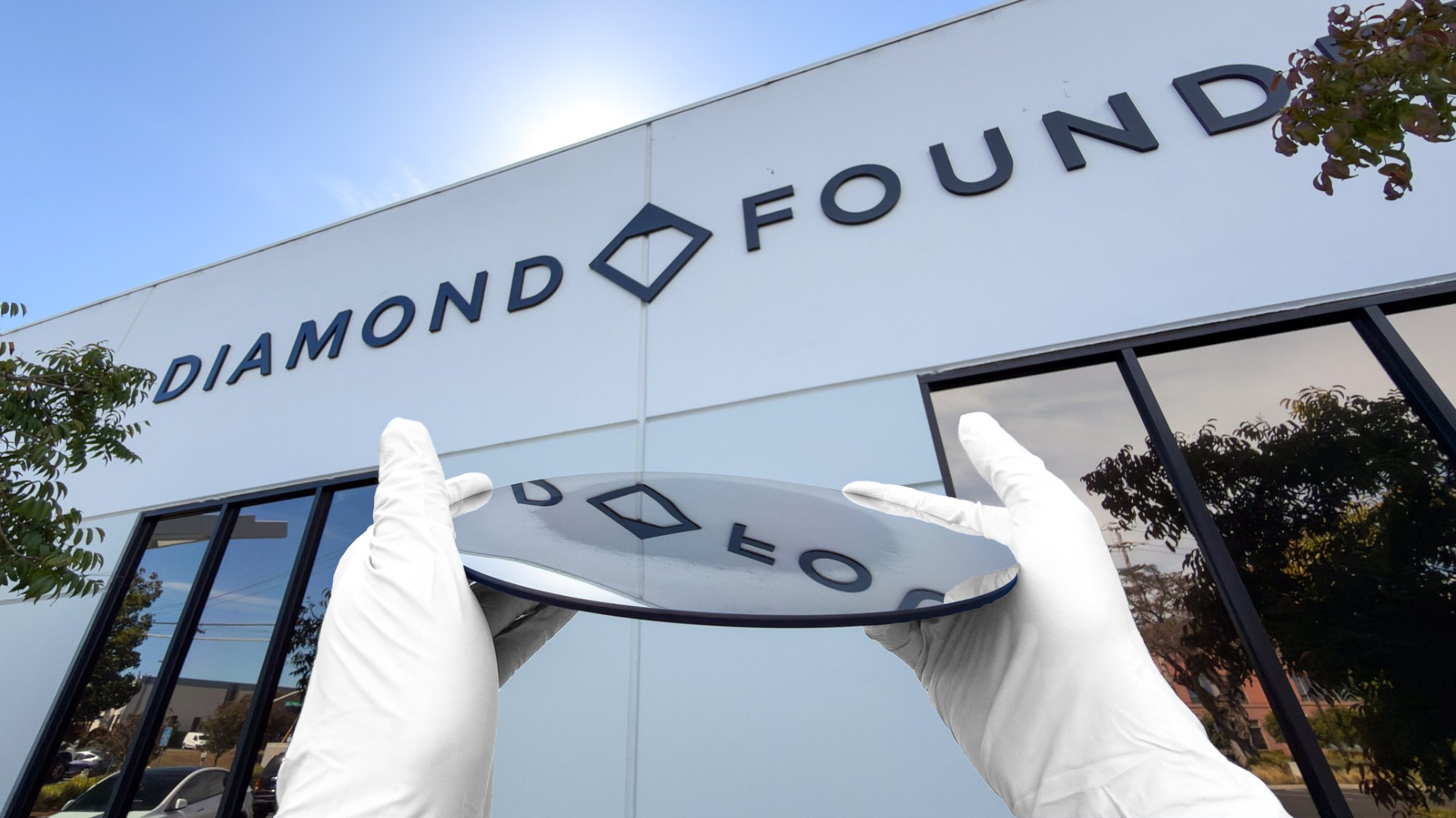
Diamond conducts heat at least five times better than copper while remaining an electrical insulator. A single-crystal wafer, unlike polycrystalline diamond, offers exactly that combination, which should reduce hotspots on a chip. The 200 mm size matches the wafers fabs use for older process nodes.
The sample shown is still unpolished and needs further processing before it suits chipmakers. The company showed a chart indicating a 300 mm wafer, the size used for leading-edge nodes, should be possible before 2030. CEO Martin Roscheisen said the milestone is the result of more than a decade of experiments, failures and rebuilt machines.
Diamond Foundry is not alone: Akash Systems received $18.2 million in CHIPS Act funding in 2024 for gallium nitride fused with synthetic diamond, De Beers is developing a copper-diamond composite, and Frore Systems is working on diamond-infused liquid cooling plates.